Calculate Crosstalk in the Time Domain
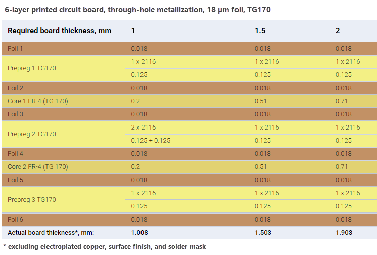
In this tutorial, we'll determine crosstalk at both the near and far ends of matched microstrip transmission lines with a solder mask. These lines connect a DDR4 memory chip and a PLD. The characteristic impedance, source impedance, and load impedance are all 40 Ohm. The lines are located on the first layer of a sample 6-layer PCB stackup (see the image below) with a thickness of 1.5 mm.
-
First, determine the trace width required to achieve a characteristic impedance of
40 Ohmfor aCoated microstrip (CM-1B)structure, as demonstrated in the Calculate Trace Width tutorial.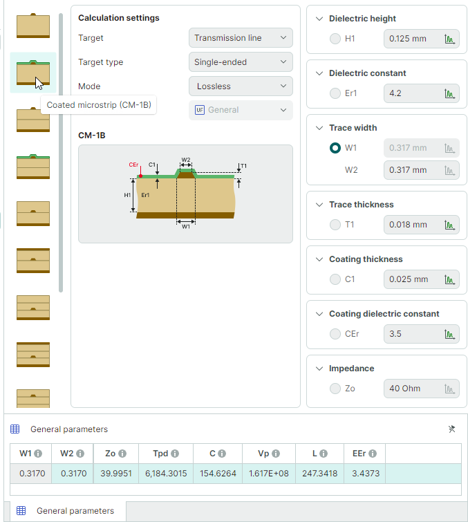
The calculated trace width is
0.3170 mm. -
In the Calculation settings panel, switch calculation mode to
Time domainand set the Parameters option toCrosstalk. The previously entered transmission line parameters will retain their values.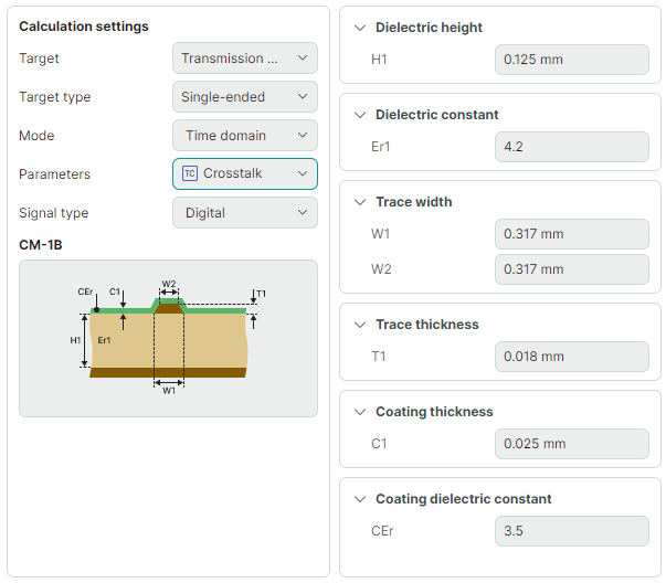
-
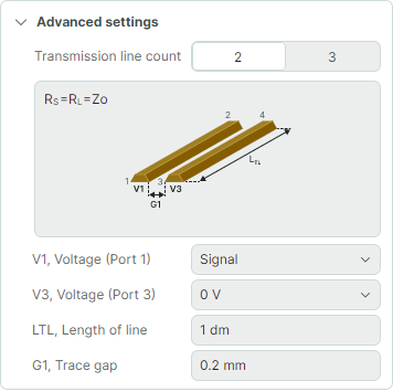
In the Advanced settings panel, set the following calculation parameters:
- Set V1, Voltage (Port 1) to
Signal - Set V3, Voltage (Port 3) to
0 V - Set LTL, Length of line to
100 mm - Set G1, Trace gap to
0.2 mm
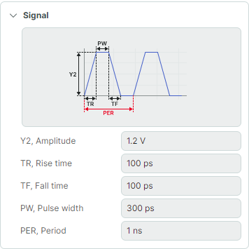
In the Signal panel, set the following signal parameters:
- Set Y2, Amplitude to
1.2 V - Set TR, Rise time to
100 ps - Set TF, Fall time to
100 ps - Set PW, Pulse width to
300 ps - Set PER, Period to
1 ns
- Set V1, Voltage (Port 1) to
-
Run the calculation.
-
To visualize crosstalk at the near end of the transmission line in the results graph, select Graphs → General parameters in the Calculation results panel. Then select
Port 3for the Port option in the View settings group box.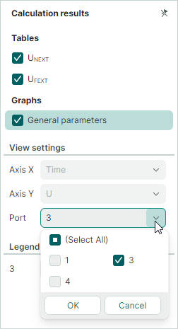
The results graph at the bottom of the window displays the crosstalk waveform at the near end of the line. The crosstalk amplitude is about
55 mV.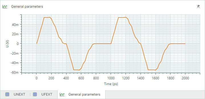
-
To visualize crosstalk at the far end of the line, select
Port 4for the Port option in the View settings group box.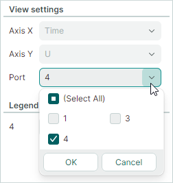
The results graph now indicates that the crosstalk amplitude at the far end of the line is about
244 mV.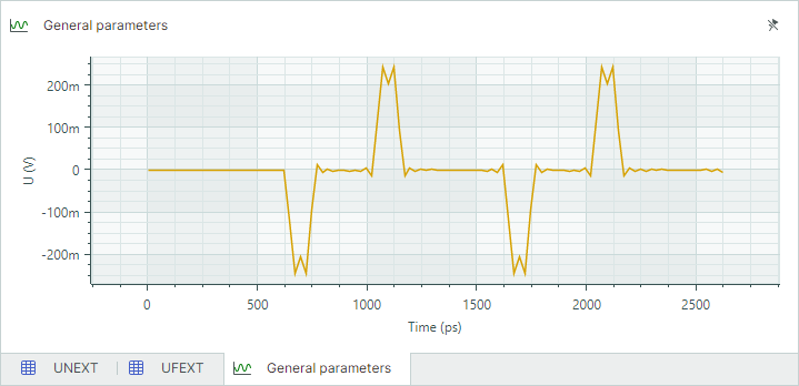
Calculations for differential transmission lines can be performed in the same way.