Calculate Differential Pair Parameters
In this tutorial, we'll calculate the differential pair parameters and secondary parameters for a differential microstrip transmission line with a solder mask. This line is located on the first layer of a sample 6-layer PCB stackup shown below. The board thickness is 1.5 mm. The reference layer is located on the second layer of the stackup. The target characteristic impedance is 100 Ohm.
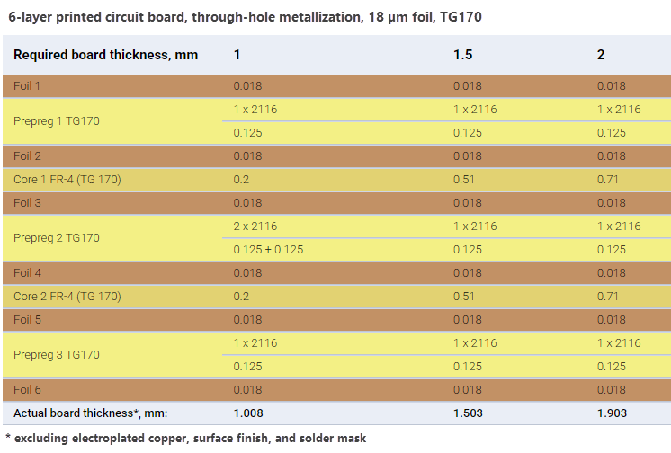
-
In the Calculation settings groupbox:
- Set Target to
Transmission line - Set Target type to
Diff pair - Set calculation mode to
Lossless - Select the
Edge-coupled coated microstrip (ECCM-1B)structure.
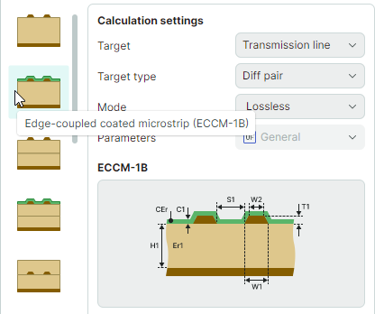
- Set Target to
-
Enter the known transmission line parameters:
- Set H1, Dielectric height () to
0.125 mm - Set T1, Trace thickness () to
0.018 mm - Set W1, Trace width and W2, Upper trace width parameters to the same value if you want to calculate the trace width without accounting for lateral undercut.
- To calculate the trace width (W1), select the radio button next to the W1 parameter.
- Set the target impedance (Zdiff) to
100 Ohm.
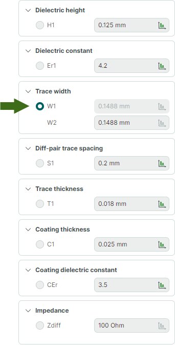
- Set H1, Dielectric height () to
-
Click Calculate to run the calculation.
The results will be displayed in a table at the bottom of the window.
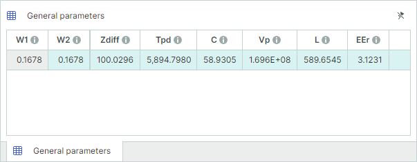
The first two columns display the calculated trace width (W1) and the upper trace width (W2). Both values are identical. The subsequent columns show the precise calculated characteristic impedance and the secondary parameters of the transmission line.
The trace width of the differential pair required to achieve a characteristic impedance of
100 Ohmis0.1678 mm.
In the same way, you can calculate the gap between the differential pair traces (S1) for a given trace width and target characteristic impedance.