Calculate Characteristic Impedance
In this tutorial, we'll calculate the characteristic impedance and secondary parameters of a stripline located on the third layer of a sample 6-layer PCB stackup shown below. The required PCB thickness is 1.5 mm.
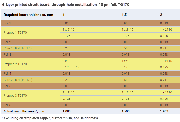
-
In the Calculation settings groupbox:
- Set Target to
Transmission Line - Set Target type to
Single-ended
Then select the
Offset stripline (OS-1B1A)structure.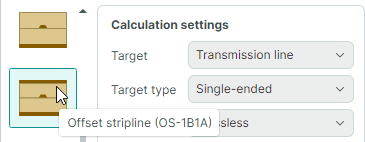
- Set Target to
-
Define the initial calculation settings.
- Select
Losslesscalculation mode. - Set the Trace inverted checkbox according to the position of the core in the selected structure.
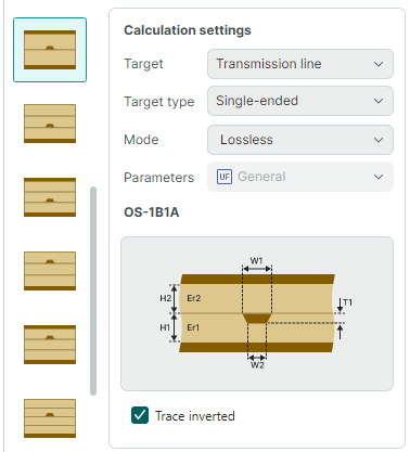
- Select
-
Enter the known geometric and electrophysical parameters of the transmission line in accordance with the target PCB stackup.
-
Set H1, Dielectric height below to
0.51 mm - Set H2, Dielectric height above to
0.125 mm - Set T1, Trace thickness to
0.018 mm -
Set W1, Trace width and W2, Upper trace width to
0.2 mm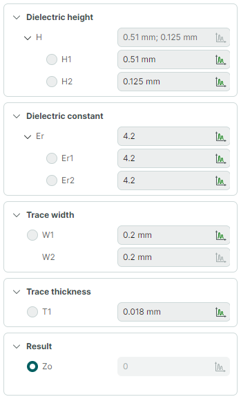
Note
Lateral undercut is not taken into account in the calculation. To account for it, you should contact the PCB manufacturer, as this parameter depends not only on the conductor geometry but also on the technological characteristics of the manufacturing process. Additionally, if the board has plated through-holes, the copper thickness on the signal layer will be greater than the nominal value. The final thickness must be agreed upon with the PCB manufacturer.
-
Click Calculate to run the calculation.
The calculation results will be displayed in a table at the bottom of the window.
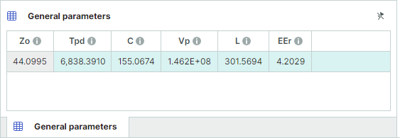
- Calculated characteristic impedance (Zo) is
44.0995 Ohm - Propagation delay (Tpd) is
6838.391 ps/m. Use this parameter for signal length matching in high-speed interfaces.
- Calculated characteristic impedance (Zo) is