Calculate Signal Waveform
This tutorial calculates a waveform after the signal passes through a matched microstrip transmission line with a solder mask. This line is located on the first layer of a sample 6-layer PCB stackup shown below. The transmission line connects a DDR4 memory chip and a PLD. The board thickness is 1.5 mm.
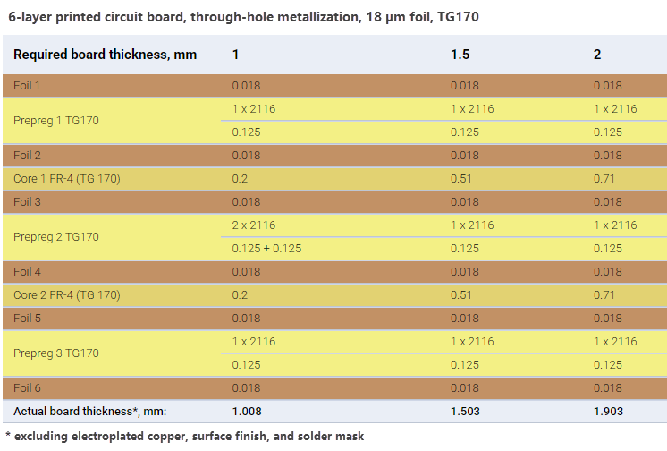
-
First, determine the trace width required to achieve a characteristic impedance of
40 Ohmfor aCoated microstrip (CM-1B)structure, as demonstrated in the Calculate Trace Width tutorial.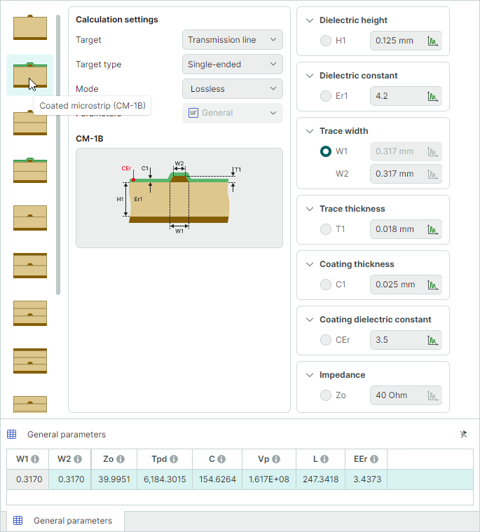
The calculated trace width is
0.3170 mm. -
In the Calculation settings panel, switch calculation mode to
Time domainand set the Parameters option toWaveform. The previously entered transmission line parameters will retain their values.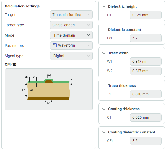
-
Set the following calculation parameters:
- Set LTL, Length of line to
100 mm - Set ZS, Source impedance to
40 Ohm - Set ZL, Load impedance to
40 Ohm - Set Y2, Amplitude to
1.2 V - Set TR, Rise time to
100 ps - Set TF, Fall time to
100 ps - Set PW, Pulse width to
300 ps - Set PER, Period to
1 ns
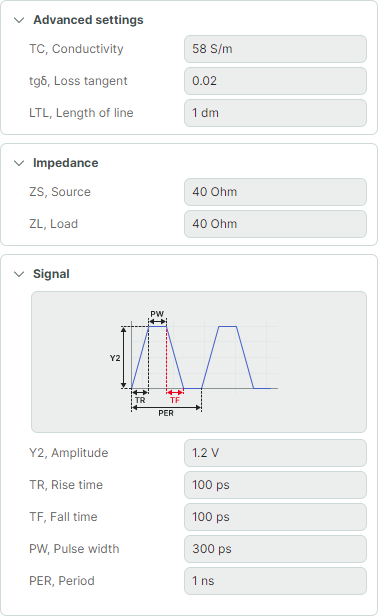
- Set LTL, Length of line to
-
Run the calculation. The results will be visualized in table and graph formats at the bottom of the window.
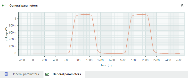
The graph shows the following information regarding the signal waveform:
- The signal amplitude has decreased to
1.1 V. - The signal rise and fall times have increased to approximately
110 ps. - The signal delay is approximately
640 ps.
- The signal amplitude has decreased to
Similar calculations can be performed for differential transmission lines. You can also use analog signals as input signals.